


AMD - XILINX FPGA最小逻辑单元CLBs, Slices和LUT区别
Author:Joe Click: Time:2023-06-26 21:56:54 From:HIZYUAN
AMD 郑重承诺支持长产品生命周期。我们很高兴正式宣布,对所有 7 系列 FPGA 和自适应 SoC 的支持将至少延长至 2035 年。这其中包括我们的成本优化型 Spartan™ 7 和 Artix™ 7 FPGA、我们的整个 Zynq™7000 SoC 产品组合,以及 Kintex™ 7 与 Virtex™ 7 FPGA。所有速率和温度等级均包含在内。
在AMD-Xilinx FPGA,用于衡量FPGA的逻辑资源的参数有CLBs, Slices和LUT等,以下是Artix-7的选型表。
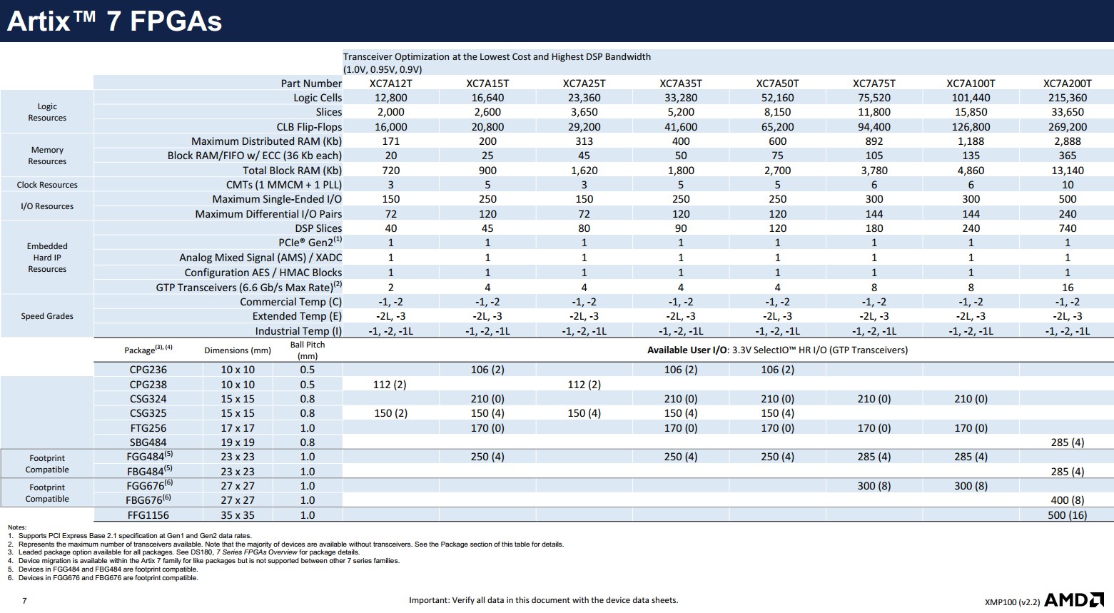
对于CLBs, Slices和LUT等这些最小逻辑单元,我们逐一做一个简单介绍:
1、LUT:
Look-up tables 查找表;Xilinx 的LUT是6输入查找表。 在器件内部的数字电路,就是通过一个个查找表实现不同的逻辑功能。
2、Slice
每个 Xilinx 7 系列 FPGA Slice 包含4个 LUT查找表 和8个触发器; 只有一些Slice 可以将其 LUT 查找表用作分布式 RAM 或 SRL。(Each 7 series FPGA slice contains four LUTs and eight flip-flops; only some slices can use their LUTs as distributed RAM or SRLs.)
每个Slice 还可以包含查找表LUT、寄存器register、进位链和多个多数选择器构成。
Microsemi的最小逻辑单元根据器件系列不同,有2个衡量单位。一是VersaTiles,它等效于一个三输入查找表或者一个D触发器;二是Logic Elements(LE),则等效于一个4输入查找表+1个D触发器。
3、CLB(Configurable Logic Block)
CLB具有以下特点:
• 6输入查找表(LUT)
• LUT 内的存储能力(Memory capability within the LUT)
• 寄存器和移位寄存器功能(Register and shift register functionality)
7 系列 FPGA 中的 LUT 可以配置为一个具有一个输出的 6 输入 LUT(64 位 ROM),也可以配置为两个具有独立输出但具有公共地址或逻辑输入的 5 输入 LUT(32 位 ROM)。 每个 LUT 输出都可以选择在带寄存器功能的触发器。 四个这样的 LUT 及其八个触发器以及多路复用器和算术进位逻辑形成一个 slice,两个 slice 形成一个可配置逻辑块 (CLB)。 每个切片的八个触发器中的四个(每个 LUT 一个)可以选择配置为锁存器。
25-50% 的 Slice 还可以将其 LUT 用作分布式 64 位 RAM 或 32 位移位寄存器 (SRL32) 或两个 16位移位寄存器(SRL16)。 当前的综合工具可以实现高效的逻辑、算术和存储器特性。
( The LUTs in 7 series FPGAs can be configured as either one 6-input LUT (64-bit ROMs) with one output, or as two 5-input LUTs (32-bit ROMs) with separate outputs but common addresses or logic inputs. Each LUT output can optionally be registered in a flip-flop. Four such LUTs and their eight flip-flops as well as multiplexers and arithmetic carry logic form a slice, and two slices form a configurable logic block (CLB). Four of the eight flip-flops per slice (one per LUT) can optionally be configured as latches.
Between 25–50% of all slices can also use their LUTs as distributed 64-bit RAM or as 32-bit shift registers (SRL32) or as two SRL16s. Modern synthesis tools take advantage of these highly efficient logic, arithmetic, and memory features.)
4、DSP slices
具有 25 x 18 乘法器、48 位累加器和预加器的 DSP 片,用于高性能滤波,包括优化的对称系数滤波。(DSP slices with 25 x 18 multiplier, 48-bit accumulator, and pre-adder for high-performance filtering, including optimized symmetric coefficient filtering.)
5、Block RAM
Block RAM 的一些主要特性包括:
• 双端口 36 Kb 块 RAM,端口宽度高达 72位
• 可编程 FIFO 逻辑
• 内置可选纠错电路
每个XILINX 7 系列 FPGA 有 5 到 1,880 个双端口块 RAM,每个 RAM 存储 36 Kb。 每个 Block RAM 都有两个完全独立的端口,它们只共享存储的数据。
以上是关于AMD FPGA的最小逻辑单元的介绍,不同的系列,芯片的资源不同,最小逻辑单元的定义是一致的。

 Jane
Jane
